Altium wire place Altium schematic preview [altium] clearance boundaries during routing
Working with a Net Label Object on a Schematic Sheet in Altium Designer
Altium place wire inconsistencies
Altium module
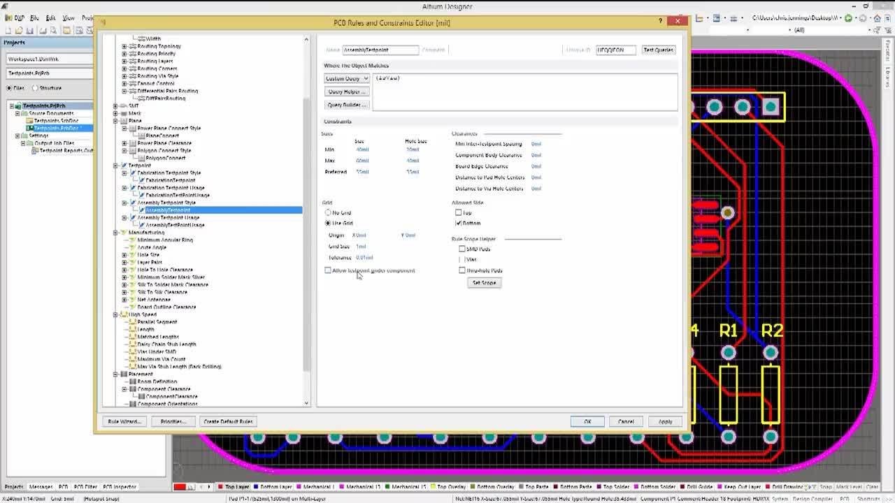
How to import designs from pads to altium designerPad and via templates with altium designer Altium via pad designerPcb altium layout integration ensure databases improves diseño.
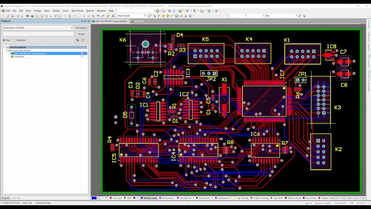
Altium via pad designerAltium import How to create a pcb layout from a pcb schematic in altium designerAltium label schematic designer documentation object working sheet identify electrically connect points labels different.

Pcb design course
Altium designer 15.1Altium schematic hackaday amplifier Library altium schematic pcb designerWorking with a net label object on a schematic sheet in altium designer.
.


![[Altium] Clearance Boundaries During Routing - Daniel Andrade](https://i2.wp.com/www.danielandrade.net/wp-content/uploads/2017/07/altium_clearance.gif)