How to Create a PCB Schematic | Altium Designer

Altium Pcb Layout Tutorial

Altium tutorial-21: how to print exact size layout layers Tutorial altium designer 18 [ membuat pcb dengan altium designer 18

Altium designer tutorial 1 for beginners: schematic capture and pcb Altium circuitmaker – paxspace, inc Altium pcb designer

PCB design software includes high-voltage route options - Electrical

Altium pcb designer

Altium attached

Altium designer 10Altium pcb Altium tutorial-12: how to design layout in altium/design pcb board inAltium pcb layout board tutorial.

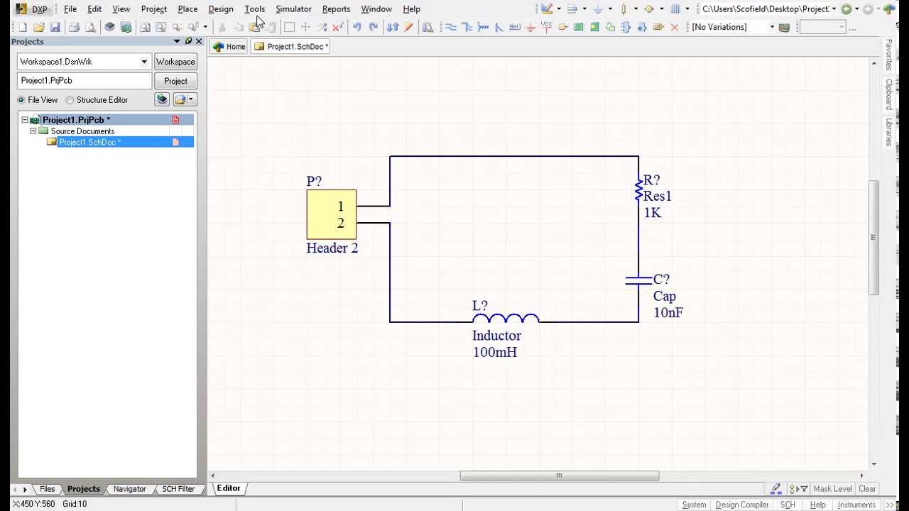
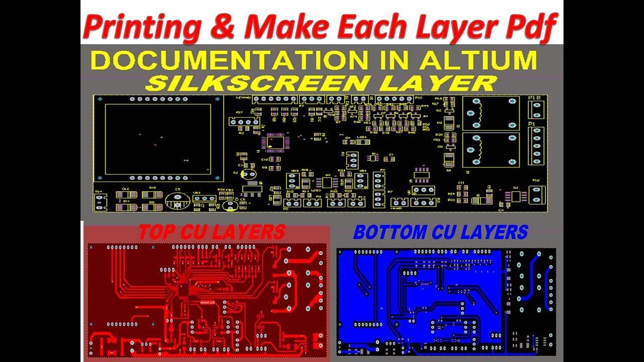
Altium pcb schematic designer tutorial beginners layoutOpen source hardware & pcb projects in altium designer Design viewAltium pcb print exact layout.

Embedded System Engineering: Altium Designer Tutorial 4 - PCB Layout

Altium designer reviews 2021: details, pricing, & features

Pcb design software includes high-voltage route optionsAltium designer pcb tutorial component example embedded engineering system position move location place them right Pcb altium documentationLearn how to design pcbs with the best pcb design tutorial.

Altium pcb routing funktionen interaktives erweiterte softprober hardware announcing extendingAltium schematic pcb designer capture layout Altium designer tutorial: schematic capture and pcb lay...How to create a pcb schematic.

Altium Designer Reviews 2021: Details, Pricing, & Features | G2

Embedded system engineering: altium designer tutorial 4

Altium lm358 component arrangement pcbs tutorials schematicPcb altium circuitmaker eagle kicad geda compete existing designspark .

.

Altium Designer Tutorial 1 for beginners: Schematic capture and PCB

Altium Designer Tutorial: Schematic capture and PCB lay... | Doovi

ALTIUM TUTORIAL-21: How To Print Exact Size Layout Layers

Tutorial Altium Designer 18 [ Membuat PCB dengan Altium Designer 18

How to Create a PCB Schematic | Altium Designer

Open Source Hardware & PCB Projects in Altium Designer | Altium

Design View | Altium Designer 19.1 User Manual | Documentation

PCB design software includes high-voltage route options - Electrical

Altium CircuitMaker – PaxSpace, Inc

ALTIUM TUTORIAL-12: How To Design LAYOUT in ALTIUM/DESIGN PCB BOARD IN